
The Saga of the Transceiver SMDs


The Development Journey, Part III

Once we got past the decoding issue we were ready to complete the graphical user interface, build a cabinet, assemble the transceiver boards and address various issues around features and operations. Phew! At that point, we had named our little Arduino QRP radio the CTX-HF3, a very techie name for such a lightweight fellow. That would change.
The photo shows the fairly complete breadboard version that would render as a control board. So what’s missing? The transceiver, of course! The first board we built was the control system for a transceiver.
That board manages band switching and band selection. While it can handle six bands: 80, 40, 20, 15, 12, and 10 meters, at this point, we have provided only a single-band transceiver PCB. We hope to add other bands soon, and maybe even a dual-band board.
We developed the transceiver board for 40 meters as a compromise, since 80 meters required an antenna that was too long for many situations, and 20 and above bands were not as good for local and regional communications as 80 and 40. Building additional single-band boards requires changing the inductors and some capacitors on the board, but we have not gotten to that yet.

QRP Tech in a box
We were also working on a box or cabinet to put the circuitry into. We purchased a 3D printer, and designed a cabinet using 3D software, and began printing our own cabinets. It turned out that they were not strong enough, and part of the reason was the printer was skipping, thus leaving small gaps and giving us a weak result.
When we finally figured it out, we were able to improve the situation but not fully correct it. In the photo, you can see the printer beginning to print a box, as it builds up the object layer by layer—frequently skipping parts of layers—but the case was very useful for where we were at the time. We were on the road to a portable CW transceiver made in the USA.
Transceiver parts like pixie dust
The next problem we had to overcome was surface mounted devices (SMD) on the PCBs. They were new to us. SMDs are extremely tiny parts soldered on the top surface of the circuit board, unlike through-hole components that are soldered on the bottom of the PCB. They are tiny, ranging down to 0.04″ x 0.02″ in size—so small that a grain of rice looks big in comparison. Back in the day at Apple, when my designs were turned into SMD, I had nothing to do with that phase of product development. Consequently, I didn’t foresee the next few wrinkles.
At first it was smooth sailing. When our first set of un-assembled control boards came in, a team member with considerable experience in SMD PCBs offered to build two. After he completed those front-panel PCBs, we buttoned up a lot of initial testing, made a few changes and headed into the second preproduction run. It was also time to design the SMD transceiver board. Our ham radio preppers were waiting.
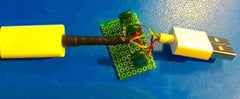
Then things got a little rough. By the time the transceiver boards were developed and ready for assembly, our guy was no longer available. Surely we could do it ourselves, we thought. Just so you have some idea of what we were dealing with, here’s a blank transceiver board alongside a paper clip. The dark spots are targets for more than 100 SMDs.
We borrowed a soldering oven, ordered all the other stuff. We were good to go. With several team members on board, we used a metal stencil to squeegee solder paste onto the board where the parts were to go. Carefully we passed out the parts, one at a time. Using tiny tweezers and microscopes or magnifying lenses, we painstakingly placed the parts where they were meant to go.
Wandering components
After placing maybe 50 components on the transceiver boards, someone noticed pieces scattering around his board and the general area. Huh? How did that happen? We had been so careful, so precise. What went wrong? We could only guess. Maybe he breathed too hard? Accidentally swished his shirt over the board when he reached for the next strip of parts?
Then the other assembler noticed the same problem. Pieces everywhere. It was already difficult enough building this sort of board. Paste was drying. This process was too time-intensive. We’d have to start over.
The stray parts were not recoverable, not these miniatures. SMD parts, especially capacitors, are not marked with values. If they were, you could only read them under a microscope. If one fell on the floor, you could kiss it goodbye because it was unlikely you would ever find it. We threw in the towel. Doing it ourselves wasn’t going to work.
Let’s give this a shot
At that point I was searching for a company to build those confounded radio PCBs, relieve the stress of dealing with the SMDs, get this 40 meter radio project back on the road. I would simply maintain the inventory and hand the rest off to someone else. Seemed straightforward.
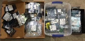
I signed up with a group that sounded reasonable enough. Until reality kicked in. On my side, simply ordering the inventory of more than 200 different parts took countless hours. After they arrived in labeled, anti-static bags, I would tally and “kit” them. Oh, yeah, then pay for shipping to a manager several hundred miles away, reimburse that person to recount them, repackage them and ship them overseas for assembly.
So I’d just handle inventory and my long-distance manager. All right? Hang on. Inventory, manage that manager, pay for shipping the lot overseas where they would be counted yet again, get the boards assembled by hand, repackaged, sent back to my long-distance manager, who would unpack, check, repack and ship the boards back to me and make it all easier, right? Not. Too much shipping expense, repeated operations, and time wasted.
No way! Forget it! Preproduction Round Number One of the transceiver boards still wasn’t working out. There had to be a better way.
Radio boards assembled and delivered!
Finally, at last, we had the first full unit, with both the main PCB, aka the front panel, and the new transceiver PCB. Preproduction Run Number Two was going well.
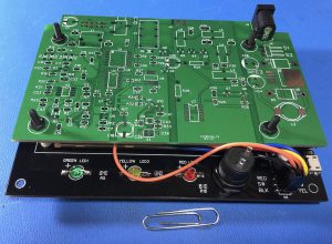
The PCB company assembled everything except the toroids. We were hand-winding them at that point and soldering them onto the PCB. In the photo you can see a completed unit showing the transceiver PCB mounted on top of the LCD PCB and the main CPU PCB.
Promise of the early 40 meter radios

Naturally, over time we found things that needed improvement, but the radio was doing all right. We shipped several units out into the field for testing, with good reports returning. The feedback coming to us recommended that we enlarge the text on the main screen, move the buttons on the display so that they were easier to touch, strengthen the case design, add a lid to protect the front panel when not in use, and more.
Around then, we also started working with the Small Business Development Center (SBDC) in Coeur d’Alene. Over time they have provided a wealth of coaching in business operations. More recently, they have added coaches for website functionality and marketing via social media, which at this writing is just getting under way.
At that point, while things were going well, we determined that 15 µv sensitivity in the receiver was not good enough. So, we prepared to develop a much more sensitive receiver—about 30 times more sensitive. We also discovered that the bandwidth of the bandpass filter was wide enough that we did not really need the tunable inductor, shown in the photo, upper left. And we designed a better band pass filter for the front end, with the help of another ham operator.